Aditya Mittal
CERN LHCb TELL1 VELO
PHY490 Independent study Report
Advisor: Marina Artuso
May 10, 2007
Table of Contents
Introduction to the TELL1
Data Acquisition Board
Common versus Detector
Specific Logic
Pedestal Subtraction and
Common Mode Suppression
Introduction to the TELL1 Data Acquisition Board
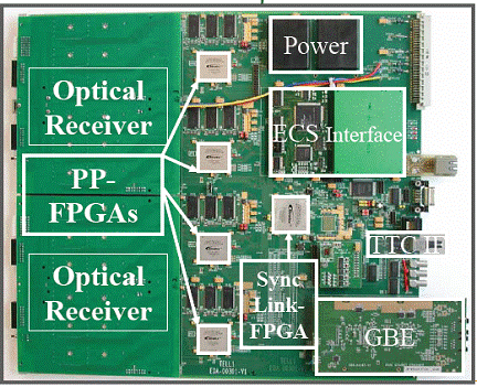
Image from http://lphe.epfl.ch/~seminar/intern/2006/potterat_24Jul2006.pdf
Shown in the picture above is the LHCb project’s TELL1 Board. This is the common data acquisition board for the TELL1. On it there are 5 Altera FPGAs. An FPGA is a FIELD PROGRAMMABLE GATE ARRAY meaning it is a system of digital gates that can be programmed to create different digital architectures. VHDL (VHSIC Hardware Description Language) is the language that we use to define the architecture that we want to synthesize onto the FPGA.
Four of the five FPGA in this board are used for pre-processing the data received by the optical receivers at the front end of the board. The fifth FPGA is the Sync-Link FPGA which is then used to accumulate all the data from the pre-processor FPGA (pp_FPGA).
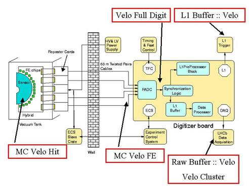
Image from http://ppewww.physics.gla.ac.uk/~parkes/VeloSoftware/EventModel.jpg
Shown above is the general setup of the board with respect to the silicon sensors at the front end that accumulate charge (measured in MeV) from particle detection. This charge from the sensor is read by front end chips known as the “Beetles.” A Beetle amplifies signals from the silicon sensors and pipelines them in a buffer which is read when an L0 accept signal is high. The L0 trigger sets the L0 accept signal.
Beetles and the Front End
Each Beetle can handle 128 detector channels. Each analog output can handle 32 channels, and so we have 4 analog outputs from each Beetle that are send some 50 to 60m to the TELL1 board in the control room over copper wire. Due to high levels of radiation, the processing cannot be done near the sensors themselves and CAT6 cables with individually shielded twisted pairs are used near the sensors. The analog links from the Beetles provide us with data at 40MHz frequency. With the TELL1 we will be outputting at only 1.11MHz frequency so we can operate all of the various sub-detectors with TELL1 being the common data acquisition board.
Common versus Detector Specific Logic
The various sub-detectors include the Vertex Locator (VELO - the one which I looked more into), Outer Tracker (OT), Silicon Tracker (ST), Ring Imaging Cherenkov counters (RICH), and Muon Detector. Additionally, there is also an L0 Trigger and a High Level Trigger (HLT) which are supported by the TELL1.
The way the TELL1 board FPGA logic is organized then is that first we put down all the things that can be made common to the various detectors, and then we put down all the things that are specific to the individual detectors need. The idea is to keep looking for and finding the blocks of logic that multiple detectors can use and making them common so we can save space on the FPGA and improve the timing of the system as well.
ADC Values
Because the data the TELL1 acquires from the sensors is analog, the first step has to be to convert this analog data to digital data for processing. This is done using the ADC (Analog to Digital Converter) on the board. What this results in is a numerical value that is linearly proportional to the voltage level resulting from the accumulated charge on the sensors on that analog wire.
FIR Correction
Once, the ADC value (the numerical output of the Analog to Digital Converter) is known, we then do FIR correction. FIR stands for finite impulse response and is a result of passing the signal through a low pass characteristic cable (the copper wires that carried the analog signal to the TELL1). Supposedly, the FIR filtering should correct the finite impulse response acquired during the transport in the signal.
Pedestal Subtraction and Common Mode Suppression
Next, we calculate and subtract a pedestal value from it which supposedly helps us eliminate local variations in the signal such as the variations due to temperature dependence. I believe the correct pedestal calculation is still debatable as simply taking the average of N events and subtracting that from the FIR corrected value is probably not sufficient for this.
I looked at the specific case for the VELO Pedestal calculation and this one is discussed in my notebook for the dates 4/5/2007 and 4/10/2007. In the VHDL code the pedestal subtraction is done by an entity called velo_PEDESTAL_calculation. This entity takes in many parameters such as a 10 bit input data, which will come from the ADC value coming into the pp-FPGA on which this pedestal calculation is being done. There are various enable signals (denoted by _en in VHDL naming scheme), header correction values (we did not discuss header here but along with the data there are also headers denoting particular information about the Beetle, these headers are also not read out during zero suppression, which is used when the bus width is limited), a zero suppression enable or disable signal, header correction enable, header correction value signals for the various strips and the address of the memories to which to read and write to are all detailed in the VHDL code.
The pedestal process architecture contains 2 processes, one that does the actual subtraction and updating, and one that scales the data after the subtraction. Scaling data does not result in better resolution, merely covering the whole range of possible digital values. The pedestal value is 10 bits wide, and the output data is 8 bits wide.
Along with the pedestal subtraction for VELO there is a state machine PP_pedestal_bank_assemble that is used by the PP_pedestal_bank_linker. Before I make this all confused, let me go back to discuss the role of the Linker.
Data Linker for TELL1
Between the four PP_FPGA and the SyncLink FPGA is the data linker for the TELL1. There are 2 parts to the data linker. The first part of the data linker is the PP_Linker and the second is the SL_Linker. The PP_Linker collects all the information inside the PP_FPGA while the SL_Linker links the information from the 4 PP_Linkers together and exports that data to be assembled as MEP. Refer to TELL1 “Internal Data Transform Protocol” by Guido Haefeli.
This PP_Linker works on a FIFO basis (first in first out like a queue) and has control and data parts. The control part includes the input source called “Info,” while the Data part supports input types “cluster,” ADC Value, Non-Zero Suppressed Data, and “Pedestal.” In the case of the VELO which is the one I was looking at the “Info,” “Cluster,” and “ADC” banks are always enabled, while “un-zero,” and “pedestal” are by default disabled but may be enabled.
The PP_Linker indicates the start of a new bank by a series of four ones, “1111.” The scheme for the ST detector is the same as that of VELO for the Linker. In the end, the SL linker puts the VELO and ST “Cluster,” and “ADC” banks into one zero-suppressed bank.
Clusterization
The reason we must use a clusterization algorithm is because a single real event may cause some charge to be accumulated on various places in the silicon detector producing multiple analog signals from the front end Beetles. The level of the signal will be high in the region of the hit and the level of the signal will be weaker in the region surrounding it.
The problem is complicated by the fact that multiple events may happen at the same instant in time. Therefore, in order to detect truly the number of events that happened, we cannot simply read digital values above a certain threshold and know. We must take into account the various scenarios of signals that can arise from the different possible event combinations. Reference [1] “LHCb VELO and ST clusterization on TELL1” describes in detail the algorithm we are using to do this clusterization. It describes “spill over information” that is information from one event that is interfering with the signal from another event and the ways in which we deal with it and also which aspects of clusterization are common to the different detectors and which are detector specific, because there might be signals that don’t bother a specific detector.
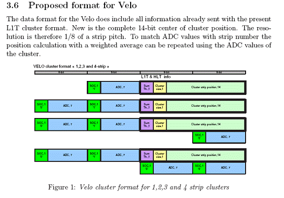
The idea is to support up to 4 strip clusters and no more. And depending upon the number of strips in the cluster we have a format for storing the cluster bank as shown to send to the linker. I explore the VHDL code that does this in my notebook. The specific module that comes up with the cluster data in VHDL is named “Velo_Cluster” and is composed of other modules that find and validate clusters and their strips, along with their size, position shift, adc value etc. and after all kinds of calculation we are able to formulate the 48 bit cluster data in the VHDL code.
VHDL Framework and Quartus II
Above I’ve described my understanding of the various facets
of what we are trying to do on TELL1.
Zero Suppression, I skipped because it is actually a rather small
implementation, although important in the VHDL code. Yesterday, May 10th, 2007, I gave
a PowerPoint presentation to our team here at
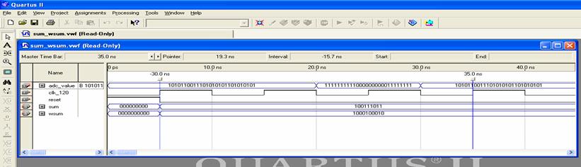
Shown above is the waveform that shows the output of the sum and wsum calculations for various ADC values. The way this calculation is being done is that the ADC value is 28 bits and so we split it into four 7 bit numbers. We then take the sum of the four 7 bit numbers to get the sum, and the wsum is the weighted sum. One can verify the outputs by using a calculator.
Shown above are the before and after pictures of my optimization. This is not a big modification but a proof of concept, that optimizing the VHDL code optimizes the gates.
Before:
Wsum = EXT(y1,10)+EXT(y3& ‘0’,10) + EXT(y2& ‘0’,10) + EXT(y3& ‘0’,10)
After:
Wsum = EXT(y1,10) + EXT(y2& ‘0’,10) + EXT(y3& “00”,10)
Apparently, the machine that generated the first line of code didn’t know it can shift twice in the same operation and so did two separate shifts, resulting in an extra addition, translating to an extra adder. When we generate the things using higher level like C, we get more and more of these extra and unnecessary things. Therefore, it is better to code at the lowest possible, but feasible level.
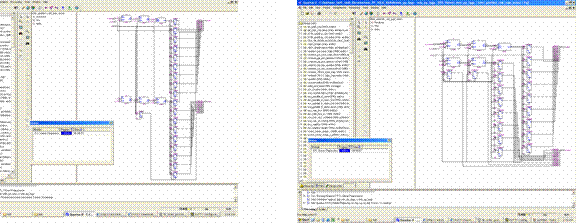
After having spent the first few days setting up, I spent some time in the Physics lab stepping through many of the blocks of code, and developing an understanding of the various modules such as clusterization, zero suppression, common mode, pedestal calculation, and the linking. Then, I figured out how to create and get waveforms with Quartus but I wanted to do a little more than that so I went off to the engineering lab to try to setup the project in the UNIX machine and run it with the Synopsis tools. I encountered a lot of trouble because I did not have enough space allocated to me on the drive, so I could not compile and use the full project.
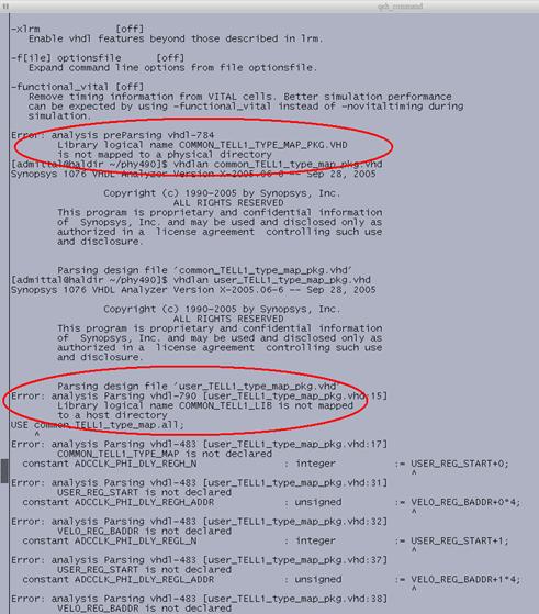
I then went ahead and sorted out the files I wanted to simulate and use. My plan was to get that to work then I would have created a lot of testbench files beyond the few that are given to do a good amount of simulations using Scirocco and other Synopsis tools to do some verification of the code as well. Even though I figured out the files and libraries I needed and included them and setup the environment and the work directory I had trouble because of these errors shown in the diagram below due to improper linking. After I spent many days trying myself, I tried to get some graduate students in engineering that are really good at these things to help me but none of us understood what was wrong, and now I am out of time, otherwise, I would continue the work to figure out how to go about it.
Regardless, it has been a pleasure to work on this project. I have learnt a lot and hopefully, I have contributed to the learning of others as well, and hope you can find someone to continue this work and they will find my report and PowerPoint useful and be able to get setup and progressing faster because of it.
Acknowledgements
Special
thanks to Dr. Marina Artuso for
providing me an opportunity to work as an independent study student with her, for
her guidance and support, and promoting my interests in the learning of science
and engineering, and maintaining an extremely caring approach.
I
would also like to thank a few of my graduate colleagues, esp. one of my TA’s
Jean Hannouche and Salil Sharma, at the engineering department for trying to
help me debug errors in setting up with Synopsis, although we couldn’t get that
to work just yet. And thanks to the rest
of the high energy physics department as well.
References
[1] Guido.Haefeli and Alex.Gong “LHCb VELO and ST clusterization on TELL1” LHCb 2005 http://eckstein.home.cern.ch/eckstein/Work/TELL1/velo_st_clusterization.pdf
[2] “Chapter1 VeLo” http://www.ucd.ie/physics/lhcb/silicon/velo_chapter.pdf
[3] Federica.Legger et al. “TELL1: a common readout board for LHCb” EPF Lausanne 2004
[4] Guido.Haefeli “TELL1 VHDL Framework User Manual” LHCb 2006.
[5] Guido.Haefeli “LHCb TELL1 VHDL firmware development guide” LHCb 2005.
[6] “Chapter3 Data processing for the VeLo: the TELL1”
[7] Guido.Haefeli and Alex.Gong “TELL1 Internal Data Transform Protocol” http://lphe.epfl.ch/~ghaefeli/Release_v1.9/hdl/processing_doc/TELL1%20internal%20data%20transform%20protocol%20.doc
[8] Guido.Haefeli “FPGA based Signal Processing for the LHCb Vertex Detector and Silicon Tracker”